|
|
(860) 593-8079
757 Main Street, Manchester, CT. 06040
|

 |
Let us quote your next design.
|
|
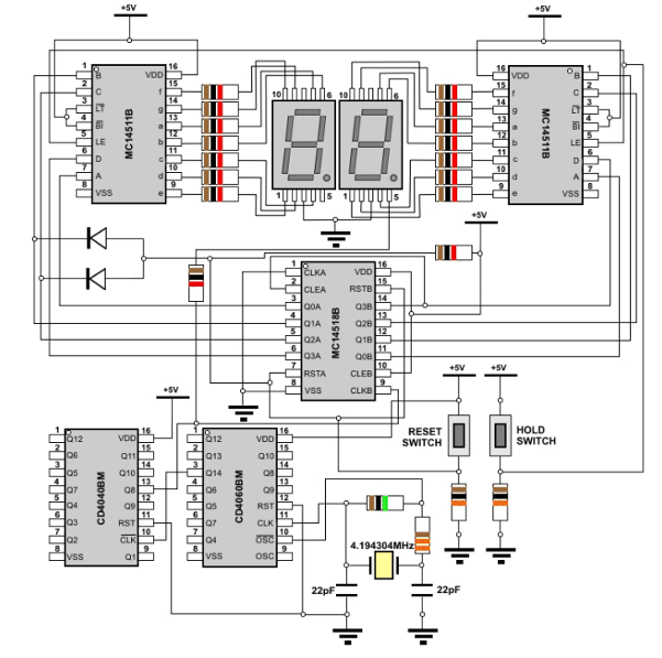
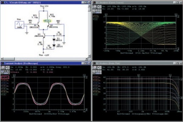
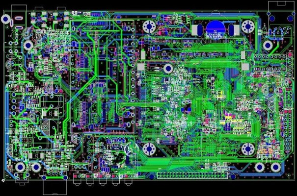
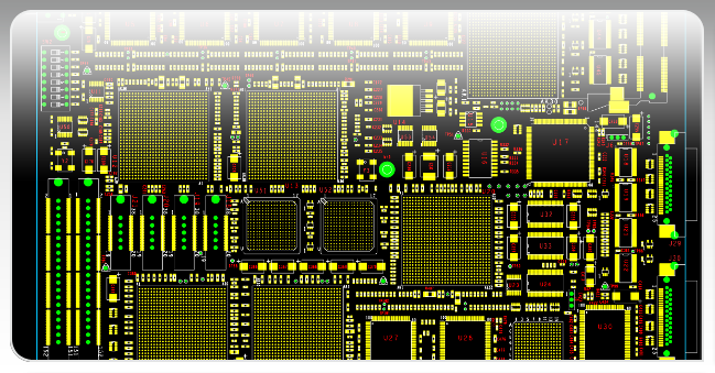
Schematic Design Schematic design or schematic entry is a step in the design cycle of electronic design automation (EDA) at which the electronic diagram, or electronic schematic of the designed electronic circuit is created by a designer. This is done interactively with the help of a schematic capture tool also known as schematic editor. The circuit design is the very first step of actual design of an electronic circuit. Typically sketches are drawn on paper, and then entered into a computer using a schematic editor. Therefore schematic entry is said to be a front-end operation of several others in the design flow. Despite the complexity of modern components - huge ball grid arrays and tiny passive components - schematic capture is easier today than it has been for many years. CAD software is easier to use and is available in full-featured expensive packages, very capable mid-range packages that sometimes have free versions and completely free versions that are either open source or directly linked to a printed circuit board fabrication company. We offer several schematic platforms to create the design. (Cadence, Orcad, Pads, NI MultiSim and Altium). Simulation Electronic circuit simulation uses mathematical models to replicate the behavior of an actual electronic device or circuit. Simulation software allows for modeling of circuit operation and is an invaluable analysis tool. Simulating a circuit’s behavior before actually building it can greatly improve design efficiency by making faulty designs known as such, and providing insight into the behavior of electronics circuit designs. The most well known analog simulator is SPICE. Probably the best known digital simulators are those based on Verilog and VHDL. Some electronics simulators integrate a schematic editor, a simulation engine, and on-screen waveforms, and make “what-if” scenarios easy and instant. They also typically contain extensive model and device libraries. These models typically include IC specific transistor models such as BSIM, generic components such as resistors, capacitors, inductors and transformers, user defined models such as controlled current and voltage sources. Printed circuit boards (PCB) design requires specific models as well, such as transmission lines for the traces and IBIS models for driving and receiving electronics. We offer several simulation platforms originally derived from the UC Berkley SPICE program to simulate and test the design before layout. PCB Layout A printed circuit board (PCB) mechanically supports and electrically connects electronic components using conductive tracks, pads and other features etched from copper sheets laminated onto a non-conductive substrate. PCBs can be single sided (one copper layer), double sided (two copper layers) or multi-layer (outer and inner layers). Multi-layer PCBs allow for much higher component density. Conductors on different layers are connected with plated-through holes called vias. Advanced PCBs may contain components - capacitors, resistors or active devices - embedded in the substrate. Printed circuit boards are used in all but the simplest electronic products. Alternatives to PCBs include wire wrap and point to point construction. PCBs require the additional design effort to lay out the circuit, but manufacturing and assembly can be automated. Manufacturing circuits with PCBs is cheaper and faster than with other wiring methods as components are mounted and wired with one single part. Furthermore, operator wiring errors are eliminated. When the board has only copper connections and no embedded components, it is more correctly called a printed wiring board (PWB) or etched wiring board. Although more accurate, the term printed wiring board has fallen into disuse. A PCB populated with electronic components is called a printed circuit assembly (PCA), printed circuit board assembly or PCB assembly (PCBA). The IPC preferred term for assembled boards is circuit card assembly and for assembled backplanes it is backplane assemblies. The term PCB is used informally both for bare and assembled boards. We offer several pcb layout platforms to create the design. (Cadence, Orcad, Pads, and NI MultiSim and Altium). |
|
|
|